 WORKING
Receipts / S12
S12 · · posted 21 Oct 2026
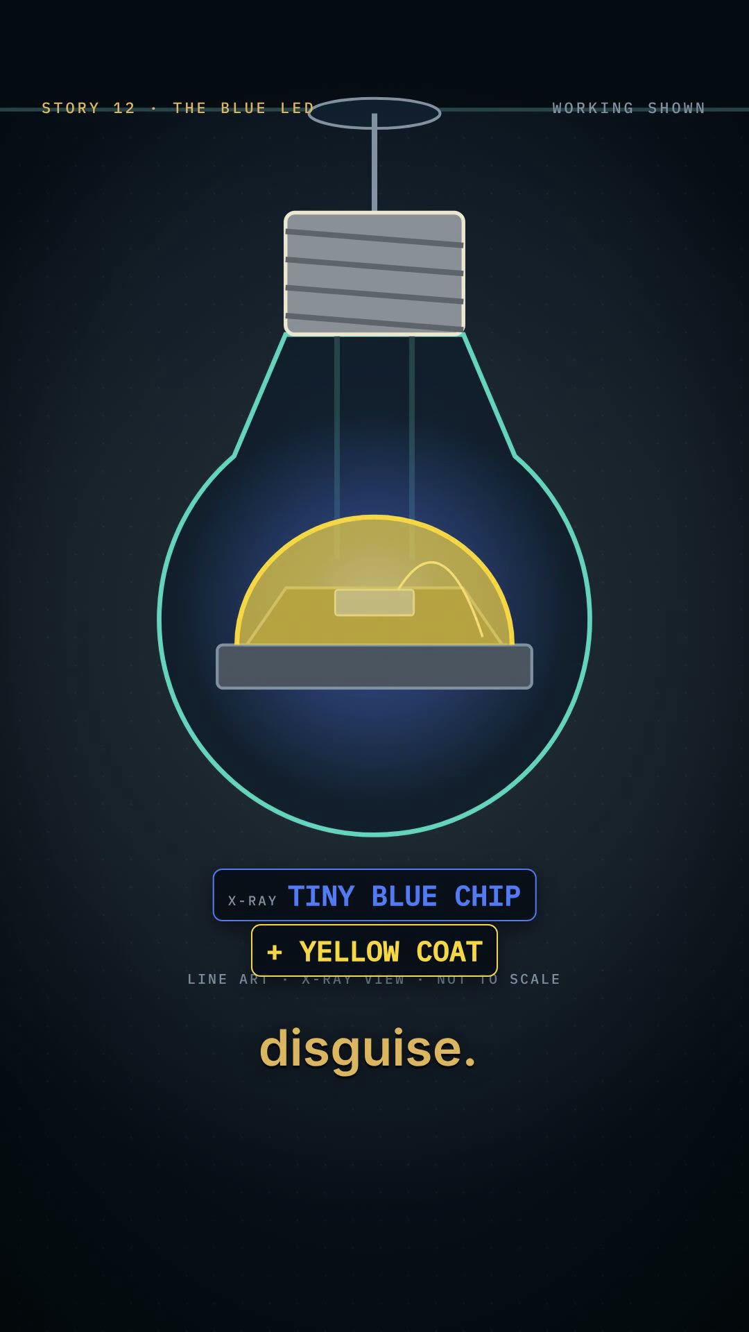
The white LED bulb above you isn't really white.
Line by line
Every claim, with its source.
Every spoken or on-screen factual claim, with the wording it rests on. Sources fetched 2026-10-11. Nobel PDFs were read with pdftotext. Currency conversions use FRED annual averages (1993 ¥111.08/$; 2005 ¥110.11/$) and are ours unless a source is quoted. Unit conversions marked "(our conversion)" are ours.
| Shot | Claim as spoken or shown | Source and verbatim support |
|---|---|---|
| hook | "The white LED bulb above you isn't really white. Inside, it's a tiny blue light in disguise." | Nakamura lecture: "Part of the blue light emitted from a blue LED is converted to lower energy colors, such as yellow, using a phosphor. The combination of blue and yellow light is perceived as white to the human eye." Sci. background: "White LEDs used for lighting are often based on efficient blue LEDs that excite a phosphor". ("Often": some white LEDs mix red, green and blue chips; true of the typical phosphor-converted bulb.) |
| hook | "And for thirty years, nobody could make that blue light bright." | Nobel press release: "the blue LED had remained a challenge for three decades. They succeeded where everyone else had failed." Sci. background: "emitting blue light proved to be a difficult task, which took three more decades to achieve". "Bright" because dim blue LEDs (SiC, GaN MIS) existed. |
| hook (screen) | "a blue chip glowing under a yellow coat" | Nichia US 5,998,925: "a fluorescent material that absorbs the light emitted by the blue light emitting diode and emits yellowish light". |
| answer | "The man who finally did it worked at a small chemical company in Japan." | Nobel press release: "Nakamura was employed at Nichia Chemicals, a small company in Tokushima". Biography: "an obscure local chemical firm"; "Nichia had fewer than 200 employees" (1979). Biography: Nichia "announced the world's first bright blue LED" (Nov 1993). "Finally did it" = the bright blue LED; the Nobel was shared with Akasaki and Amano (shown later). |
| answer | "His reward for the key patent: twenty thousand yen. About a hundred and eighty dollars." | Physics World 2002: the court noted he "received ¥20,000 in reward" for the disputed (two-flow) patent. LEDinside: "20,000 Japanese yen (US $180)"; Nichia's Akutagawa: "Nichia's payment of 20,000 Japanese yen for Nakamura's blue LED patent in the 1990s is considered generous". ¥20,000 ÷ ¥111.08/$ (1993) ≈ $180 (our conversion). |
| answer (screen) | "Map: Tokushima, Shikoku" | Press release: "a small company in Tokushima". (Tokushima is on Shikoku: geography, not quoted.) |
| answer (screen) | "¥20,000 ≈ $180 (1993)" | As above; 1993 FRED annual rate (our conversion). |
| colour | "An LED's colour is set by its material: how big a jump its electrons make." | Nakamura lecture: "The resulting photon has an energy approximately equal to the bandgap of the active layer material. Modifying the bandgap of the active layer creates photons of different energies." |
| colour | "Red is a small jump. Green, a bigger one. Blue needs a huge one," | Sci. background: GaAs "1.4 eV corresponding to light in the infrared"; GaP (red to green) "2.2 eV"; GaN "a direct bandgap of 3.4 eV, corresponding to a wavelength in the ultraviolet". Blue (450 nm) ≈ 2.8 eV via λ ≈ 1240/E (our arithmetic). |
| colour | "and the material for that was a nightmare to grow." | Amano lecture: sapphire mismatch "up to 16%"; "a mismatch of 16% should make it almost impossible". Nakamura lecture: "Either no growth of GaN occurred or the grown layer was black." Biography: GaN "was almost universally perceived to be a dead end." |
| colour (screen) | "BANDGAP ↑ = BLUE" | Nakamura lecture (bandgap sets photon energy); higher energy = shorter wavelength (standard physics). |
| colour (screen) | "Red and green LEDs lit; blue slot empty ('1960s → ?')" | Press release: "Red and green diodes had been around for a long time but without blue light, white lamps could not be created." Sci. background: red and green GaP LEDs by "a number of manufacturers" by the late 1960s. Caveat: "empty" means no bright blue; dim blue LEDs existed from the 1970s. |
| crowd | "Most researchers bet on a material called zinc selenide." | Popular info: "Nakamura at Nichia also chose gallium nitride before the alternative, zinc selenide". Nakamura lecture: "approximately 500 individuals attending the ZnSe sessions, whereas for GaN, there were around 5"; researchers said "GaN has no future". |
| crowd | "At one conference in nineteen ninety-two, about five hundred people went to those talks. About five went to hear about gallium nitride..." | Nakamura lecture: at the 1992 JSAP conference "there were approximately 500 individuals attending the ZnSe sessions, whereas for GaN, there were around 5". |
| crowd | "three of them future Nobel winners." | Nakamura lecture: the ~5 included "the chair Professor Isamu Akasaki, speaker Hiroshi Amano and myself". Press release (2014): prize to all three. |
| crowd (screen) | "ZnSe ≈ 500 · GaN ≈ 5 · three glow gold" | As above. |
| nagoya | "Two of them were in Nagoya: Isamu Akasaki and his student Hiroshi Amano." | Amano lecture: "Professor Akasaki moved from MRIT to Nagoya University in 1981"; Amano was "a 24-year-old master's student". |
| nagoya | "In nineteen eighty-five, they finally grew good gallium nitride crystals." | Akasaki lecture: "we developed low-temperature (LT-) buffer layer technology in 1985". Amano lecture: the sample came out "perfectly smooth ... and perfectly transparent". Sci. background: low-temperature AlN buffer, then GaN (published 1986). |
| nagoya | "In eighty-nine, they made a layer many thought impossible: one that carries holes instead of electrons." | Amano lecture: "it was believed to be impossible to grow p-type GaN because of self-compensation"; "we finally recognized that we had achieved p-type GaN for the first time in the world". Akasaki lecture: "theoretical studies indicated the impossibility of achieving p-type conduction in wide-bandgap semiconductors such as GaN and ZnSe"; first GaN p-n junction LED "was demonstrated in 1989". Paper: Amano et al., Jpn. J. Appl. Phys. 28, L2112 (1989). |
| nagoya (screen) | "murky → clear (1985) · P-TYPE GaN · 1989 · electron beam icon" | As above; electron beam = low-energy electron-beam irradiation (LEEBI), Amano lecture; sci. background: "Electron beams dissociate these complexes and activate the acceptors." |
| nichia | "The third was Shuji Nakamura, at Nichia, a phosphor maker in Tokushima." | Biography: "The firm made phosphors for color televisions and fluorescent lamps." Press release: "a small company in Tokushima". |
| nichia | "No PhD." | Nakamura lecture: "My only objective was to get a Ph.D. That's it." (He had none while at Nichia in this period; the dossier states it, no line says "no PhD" verbatim.) |
| nichia | "In ten years there, not one published paper." | Biography: "In ten years, Shuji had not published a single scientific paper". |
| nichia | "And he picked the material most had written off." | Biography: GaN "had been thoroughly investigated by RCA, Bell Labs, and Matsushita. It was almost universally perceived to be a dead end." Amano lecture: "MRIT decided to abandon its project on GaN-based blue LEDs". "Most", not "everyone": Akasaki and Amano (just shown) had not given up; cf. the 1992 conference, ~500 at ZnSe talks vs ~5 at GaN (crowd). |
| nichia (screen) | "PhD ✕ · PAPERS: 0 (10 YRS)" | As above. |
| reactor | "He bought a two-million-dollar machine to grow the crystals." | Nakamura lecture: "I purchased a commercially available MOCVD reactor for 2 million U.S. dollars." (His account; Nichia's money: biography, Ogawa funded the project.) |
| reactor | "It made black junk." | Nakamura lecture: "Either no growth of GaN occurred or the grown layer was black. GaN should be transparent." |
| reactor | "So for a year and a half, he rebuilt it every morning, and tested it every afternoon." | Nakamura lecture: "For the next 1.5 years, I modified the reactor design. In the morning, I would go to work and modify the reactor. In the afternoon, I would perform a couple of growths". Biography: "'remodel in the morning, experiment in the afternoon.'" |
| reactor (screen) | "BLACK · AM rebuild / PM test · 18 MONTHS · CLEAR" | As above; 1.5 years = 18 months. "Clear" = transparent GaN after the two-flow redesign (lecture: "This was the most important breakthrough in my life"). |
| heat | "Then, in December nineteen ninety-one, he tried something simple. Plain heat. And it worked." | Biography: "Shuji speculated that it was merely heat that turned the material p-type. In December 1991, he tried annealing magnesium-doped films. The resultant material was p-type." Sci. background: "Nakamura showed that even a simple thermal treatment (annealing) leads to efficient activation of Mg acceptors". Amano: "Today, almost all LED companies use thermal annealing." |
| heat | "The thing blocking those hole-carrying layers turned out to be hydrogen, trapped in the crystal," | Sci. background: "Acceptors such as Mg or Zn form complexes with hydrogen and thus become passive." Nakamura lecture: hydrogen from ammonia forms Mg-H complexes. ("Turned out": the hydrogen explanation was published in 1992, after the December 1991 annealing.) |
| heat | "and heat drives it out." | Nakamura lecture: "Thermal annealing ... above approximately 400 °C permits hydrogen to diffuse out of the crystal". |
| heat (screen) | "H atoms on Mg; heat >400 °C (752 °F); layer turns p-type" | Nakamura lecture: "above approximately 400 °C". 400 °C = 752 °F (our conversion). |
| bright | "November nineteen ninety-three: Nichia announces a blue LED bright enough to see in daylight," | Biography: "On November 29, 1993, at a press conference in Tokyo, Nichia announced the world's first bright blue LED"; the device was "bright enough to be clearly seen in broad daylight". |
| bright | "a hundred times brighter than the older blue ones." | Biography: "a hundred times brighter than silicon carbide blue LEDs". ("Older blue ones" = SiC blue LEDs.) |
| bright | "The first reaction was disbelief." | Biography: "The initial reaction was incredulity." |
| bright (screen) | "×100 BRIGHTER" | Biography, as above. |
| white | "Coat that blue chip in a yellow phosphor. Some blue gets through, some turns yellow, and your eye adds them up... as white." | Nakamura lecture: "Part of the blue light emitted from a blue LED is converted to lower energy colors, such as yellow, using a phosphor. The combination of blue and yellow light is perceived as white to the human eye." Lecture: "In 1996, Nichia Chemical Corporation developed the first white LED using the efficient blue InGaN QW DH LED and YAG phosphors". |
| white | "It gives up to ten times more light per watt than an old bulb." | Sci. background: "these new white light sources require ten times less energy than ordinary light bulbs". Press release: "just over 300 lm/W, which can be compared to 16 for regular light bulbs" (a lab record; "up to"). |
| white (screen) | "yellow YAG coat" | Nichia US 5,998,925: "yttrium-aluminum-garnet fluorescent material, activated with cerium". |
| white (screen) | "Spectrum: blue spike + yellow hump" | Measured white-LED spectrum (Deglr6328, CC BY-SA 3.0) or our own redraw: "GaN or InGaN LED" peak ~460 nm plus "Ce:YAG" band. |
| white (screen) | "~10× LESS ENERGY THAN INCANDESCENT" | Sci. background: "require ten times less energy than ordinary light bulbs". |
| bonus | "His reward? Nichia paid ten thousand yen when a patent was filed, and ten thousand more when it was granted. So, twenty thousand." | Physics World 2002: "When Nakamura filed each of the dozens of patents that he authored while at Nichia he received ¥10,000 (about £50) and the same amount when they were granted". Compound Semiconductor 2004: "paid 20,000 yen for each of the many patents". |
| bonus | "He left in nineteen ninety-nine, and sued." | Biography: "In December 1999, Shuji left Nichia". Physics World 2002: he filed on "23 August" 2001 asking ¥2bn. (Sued in 2001, after leaving; the line compresses the gap.) |
| bonus (screen) | "Two ¥10,000 notes" | As above (¥10,000 + ¥10,000). |
| court | "In two thousand four, a Tokyo court awarded him twenty billion yen." | Compound Semiconductor, 2 Feb 2004: Tokyo District Court, Nichia to pay "20 billion yen ($189 million)"; the patents could have earned Nichia "120.8 billion yen"; his contribution "not less than 50%"; the judge "awarded Nakamura the 20 billion yen that he had requested" (the court valued his share higher, but ¥20bn was what he asked for). |
| court | "On appeal, they settled for about eight hundred and forty million." | Compound Semiconductor, 11 Jan 2005: Tokyo High Court-mediated settlement, "¥840 million ($8.1 million)", incl. "The extra ¥230 million is compensation for delayed payment". AFP/Rappler: "844 million yen in 2005". |
| court (screen) | "¥20,000 → ¥20,000,000,000 (2004) → ¥840,000,000 (2005, ≈ $8M)" | As above. $8.1m (Compound Semiconductor, spot rate); ≈ $7.6m at the 2005 FRED average (our conversion); "≈ $8M" covers both. |
| nobel | "In twenty fourteen, all three, Akasaki, Amano and Nakamura, shared the Nobel Prize in Physics." | Press release, 7 Oct 2014: prize shared equally by Akasaki, Amano and Nakamura. |
| nobel | "For a blue light." | Press release: "for the invention of efficient blue light-emitting diodes which has enabled bright and energy-saving white light sources". |
| nobel (screen) | "'efficient blue light-emitting diodes'" | Press release, verbatim fragment. |
| close | "That white light is a blue chip wearing a yellow coat," | As in white (typical phosphor-converted white LED). |
| close | "and twenty thousand yen of thanks." | As in bonus (¥20,000 per patent). Rhetorical. |
What the drawing simplifies
- The LED bulb, X-ray view, energy ladder, conference rooms, factory, reactor diagram, crystal lattice, press-conference flash, banknotes, lawsuit papers and medals are our own illustrative animation. The reactor is generic line art of a two-flow MOCVD idea, not Nakamura's machine (the lecture's Fig. 4 is AIP-copyrighted and not used).
- No free photo of Nichia, its Tokushima lab, or the 1993 Nichia blue LED chip exists; the factory is line art.
- The blue LED photo (Gussisaurio, CC BY-SA 3.0) shows modern generic 5 mm blue LEDs, never "the first one".
- The white LED spectrum (Deglr6328, CC BY-SA 3.0) is a measured spectrum of a generic white LED, intensity not calibrated. If redrawn from it, the redraw must stay CC BY-SA; a fresh plot from the sources' description is our own art.
- Nakamura photo (Glenn Beltz, CC BY 2.0): UCSB, 30 Oct 2014, after the Nobel announcement, not his Nichia years.
- Trio photo (Embassy of Japan in Sweden, CC BY 4.0): Stockholm, 8 Dec 2014; tiny (280×210), small card only.
- No solo photos of Akasaki or Amano are used.
Checked, and cut
- "Nichia ordered him to stop / he threw the memos in the bin": not used (not in his Nobel texts; bin detail unverified).
- "He worked alone / invented it alone": not said; Akasaki and Amano are credited for the buffer layer and first p-type GaN.
- "Blue LEDs were thought impossible": not said; "nobody could make that blue light bright" and "a layer many thought impossible" (p-type GaN).
- "Every white light in your house is secretly blue": not said; "the white LED bulb above you".
- "A court awarded him $189 million" without the settlement: the ¥840 million settlement is always paired.
- Nichia's funding in yen (¥500m vs ¥300m conflict): not used.
- "300 lm/W" lab record, lifetimes (100,000 h), share of world electricity: checked, not used.
- "Big companies spent billions": not said.
- "Nichia is tiny today": "small" applies to the era only (under 200 staff in 1979).
Sources
Found an error?
Tell us at hello@workingshown.xyz or in the comments. We check it against the sources, pin the correction, fix the caption, and log it on the corrections page.